About
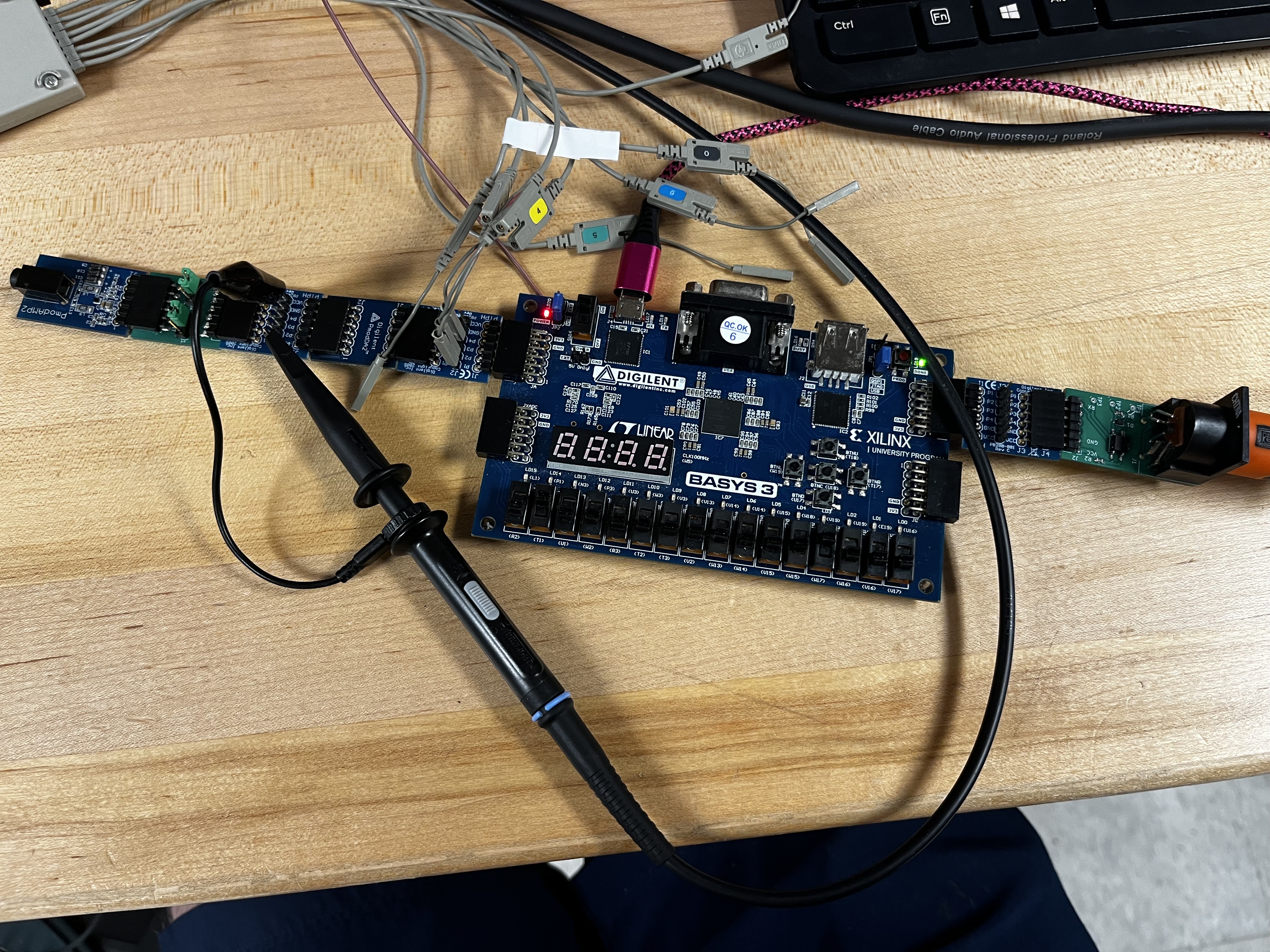
For my digital electronics class, my lab partner and I designed an MIDI controller for the Basys3 FPGA board. The FPGA was programed using VHDL. The controller acts as a receiver for the serial MIDI signal coming through over UART and does Direct Digital Synthesis (DDS) to output an analog sine wave. We both learned a lot about digital design and spent many hours debugging on an oscilliscope.
Demonstration
Source Code
Design
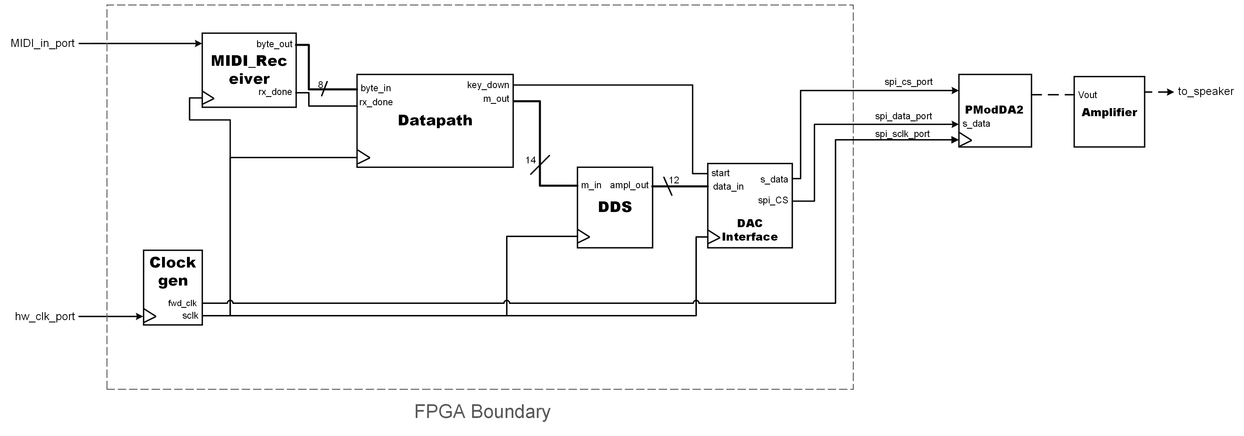
A High-Level Block Diagram of the System
Before we even started thinking about writing HDL code for the board, there were many iterations of designs on paper. Here I will go over the design of each subcomponent in the system:
Clock_gen
The Clock_Gen component generates a 1 MHz clock signal using the hardware clock which runs at 100 MHz. This system clock frequency was chosen according to the recommended specifications of the PMOD DA2 component. The maximum clock speed for the DA2 is 30 MHz, and the 1 MHz clock fits well into these specifications.
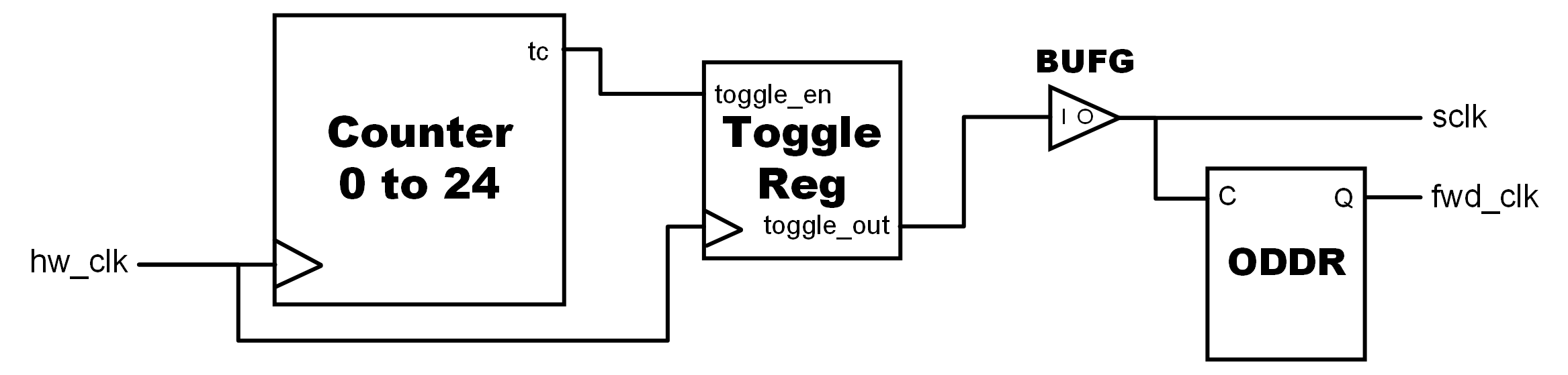
RTL Block Diagram for the Clock_gen subcomponent
MIDI_Receiver
The MIDI receiver takes the 10-bit serial data from the port MIDI_in, synchronizes it to the specified baud rate, and provides parallel out an 8-bit data_out signal to pipe into the datapath. Internally, it uses a shift register to store each bit serially, and asserts a signal once all the entire MIDI message byte has been received.
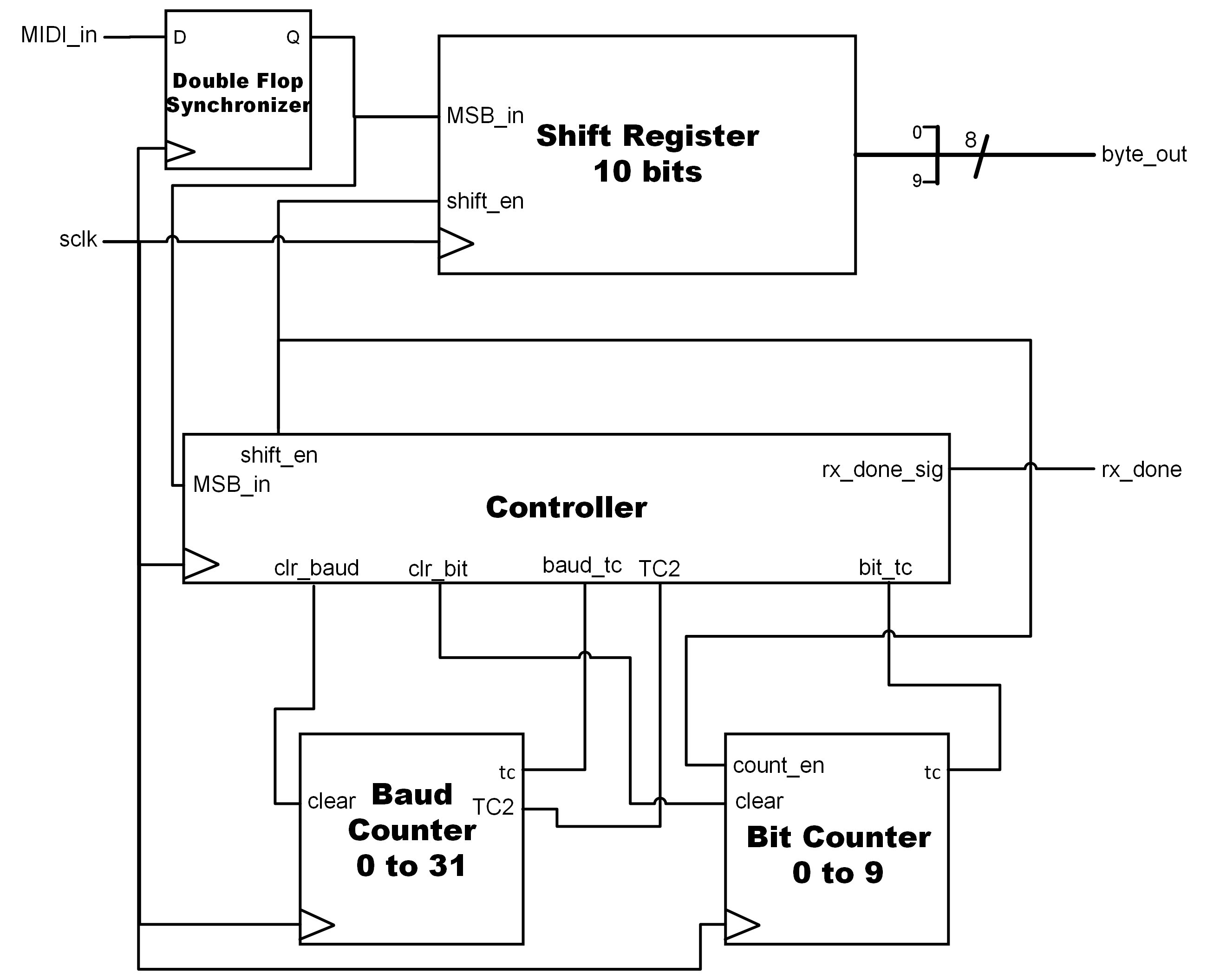
RTL Block Diagram for the MIDI_Receiver component
Datapath
The datapath receives bytes of data from the MIDI receiver one byte at a time, and stores these bytes in specified registers according to their type, whether it be a status byte, pitch byte, or a velocity byte. The datapath processes this data, and passes the necessary information to the DDS and DAC components.
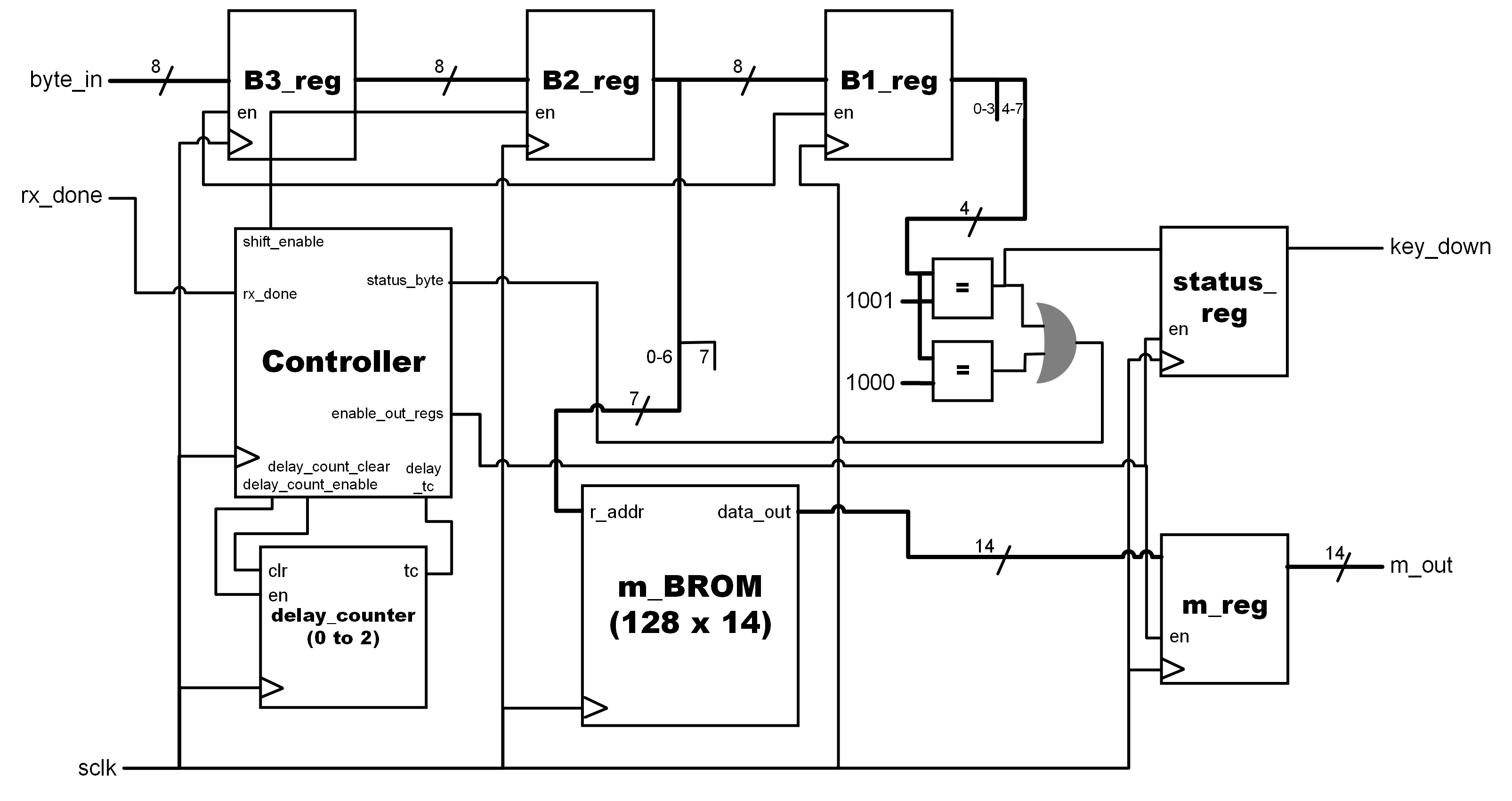
RTL Block Diagram for the Datapath component
DDS
The Direct Digital Synthesis component converts the m value (derived from the MIDI pitch number) and outputs a sine wave at the correct frequency. The sample rate is approx. 44.1 kHz (de-facto 43.8kHz), typical for cd-quality audio. The sine wave amplitudes are sampled from a BROM lookup table which was provided by Xilinx. A counter which counts by m each time specifies the output frequency (higher m means a higher frequency).
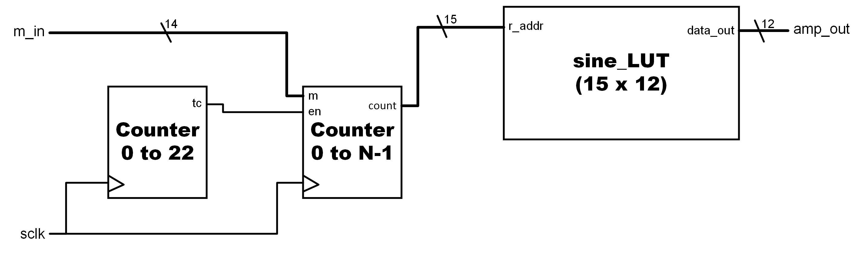
RTL Block Diagram for the DDS component
DAC_interface
The DAC Interface controls communication from the FPGA to the external PMOD DA2 component. It is a serial peripheral interface (SPI). It consists of a parallel to serial shift register and a controller. The controller asserts CS’ to the external DAC. The specific digital to analog protocol used in this design is 16 bits in big-endian with four leading zeroes.
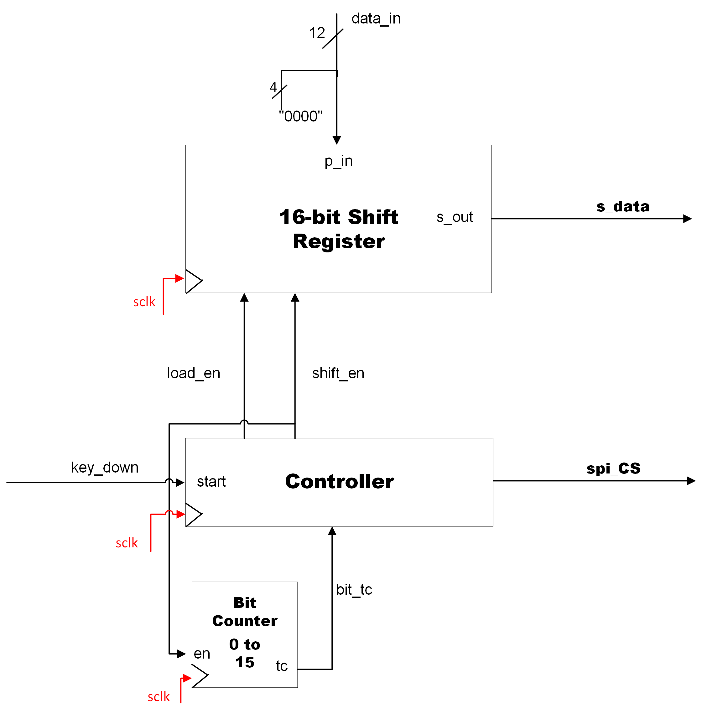
RTL Block Diagram for the DAC_interface component