Summary of Device
This device meter measures three decades of capacitance from 5 nF to 5 µF. The capacitance is outputted as a simple voltage on the range of 0.5 V to 5 V which can be easily read by a multimeter. LEDs on the breadboard display which decade of capacitance is currently being measured.
Table of Components
| Component | Value | Count |
|---|---|---|
| MAX4066 - Quad Analog Switch | N/A | 1 |
| LF412 - Dual Op-Amp | N/A | 4 |
| CD4001B - Digital NOR Logic Gate | N/A | 1 |
| CD4011 - Digital NAND Logic Gate | N/A | 1 |
| LM393 - Dual Comparator | N/A | 1 |
| Resistor | 1 kΩ | 3 |
| Resistor | 3.3 kΩ | 1 |
| Resistor | 4.7 kΩ | 2 |
| Resistor | 10 kΩ | 8 |
| Resistor | 22.5 kΩ | 3 |
| Resistor | 100 kΩ | 2 |
| Resistor | 1 MΩ | 3 |
| Capacitor | 1 nF | 1 |
| Capacitor | 4.7 nF | 1 |
| Capacitor | 10 µF | 3 |
| Capacitor | 100 µF | 1 |
How it Works
At its core, the device takes advantage of the simple law of capacitors:
$$ I = C (dV / dt) $$
Thus, if we keep $dV / dt$ constant, the current through the capacitor will be proportional to the capacitance. Using this fact, we can use a trans-impedance oscillator (TIA) to convert the current to a voltage.
For this project, we were only allowed to input a steady voltage supply. Therefore, $dV / dt = 0$, and there would be no way to measure capacitance using this input. Therefore, we built multiple Wien bridge oscillators which convert a power supply to a sine wave. Thus, $dV / dt = \omega cos(\omega t)$, and we have a sinusoidal current whose amplitude is proportional to capacitance.
Since we want the output voltage to be a steady value proportional to the capacitance, the sinusoidal voltage from the TIA must be transformed. We built a Precision Peak detector to measure the peak of the oscillating signal, with a high RC time constant to keep it at a steady value.
Missing from this summary is the digital switching logic, and the various gain/loss amplifiers necessary to keep the voltage in the correct range for both our output signal, and the specifications of the various components used in the device. Later, I will go into depth on these ommitted details.
Digital Switching
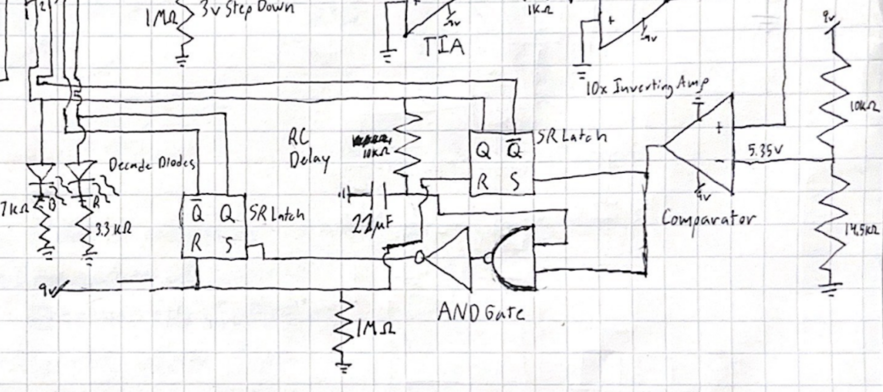
Paper Schematic of the Digital Logic Block
The device used a comparator, two SR latches, a reset button, and a quad analog switch to implement the digital switching logic for the three decades of capacitance.
The SR latches (implemented with digital NOR gates), hold their state and determine the current decade. One SR latch selects the oscillation frequency (either $\omega = 10k$ or $\omega = 1k$), and the other selects the gain (either 10x or 1x). The comparator was set with a reference voltage of 5.35 V, meaning that it would output HIGH when the input voltage (from the precision peak detector) was above this reference. The reset button resets the SR latches to their default state – measuring the lowest decade.
The comparator output, with a reference voltage of 5.35 volts, controls when the device measures a higher decade. It first increases the gain, and then the oscillation frequency. There is an RC delay between the SR latches to make sure that the device doesn’t “jump up” two decades at once.
LEDs connected to the SR latches output the current decade.
Design Methodology
With this project, I learned to move from a paper design, to a working simulation in LTSpice, to a prototype on a breadboard.
Paper Design
We started with a high-level block diagram of the various components, making sure to note the required specifications of each block.

Block Diagram Schematic for the Device
Next, we elaborated on each block to show individual circuit components and their specific values.
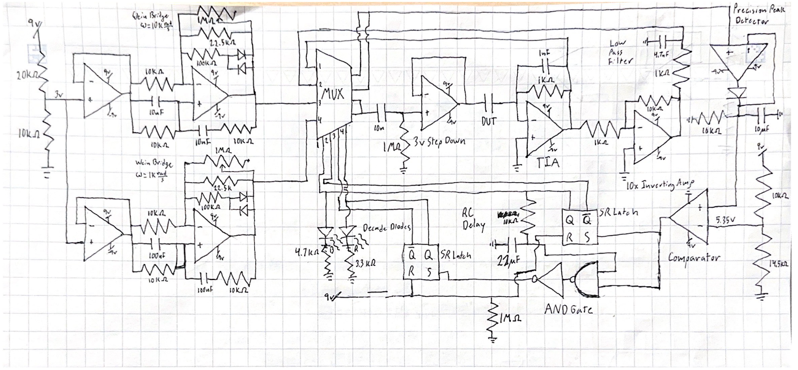
Elaborated Paper Schematic
Software Simulations
After laying out our design on paper we implemented it in LTSpice.
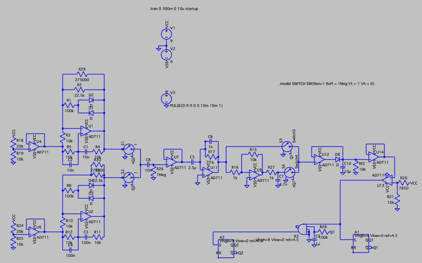
LTSpice Circuit Implementation
Now that the design was in the circuit simulation software, we could test it with various capacitance values to test its performance.
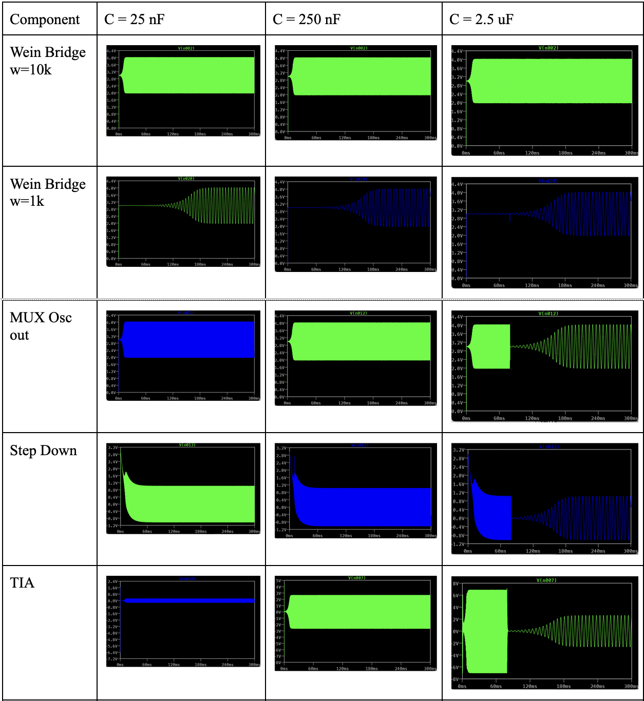
Example Simulations From LTSpice with Different Capacitance Values
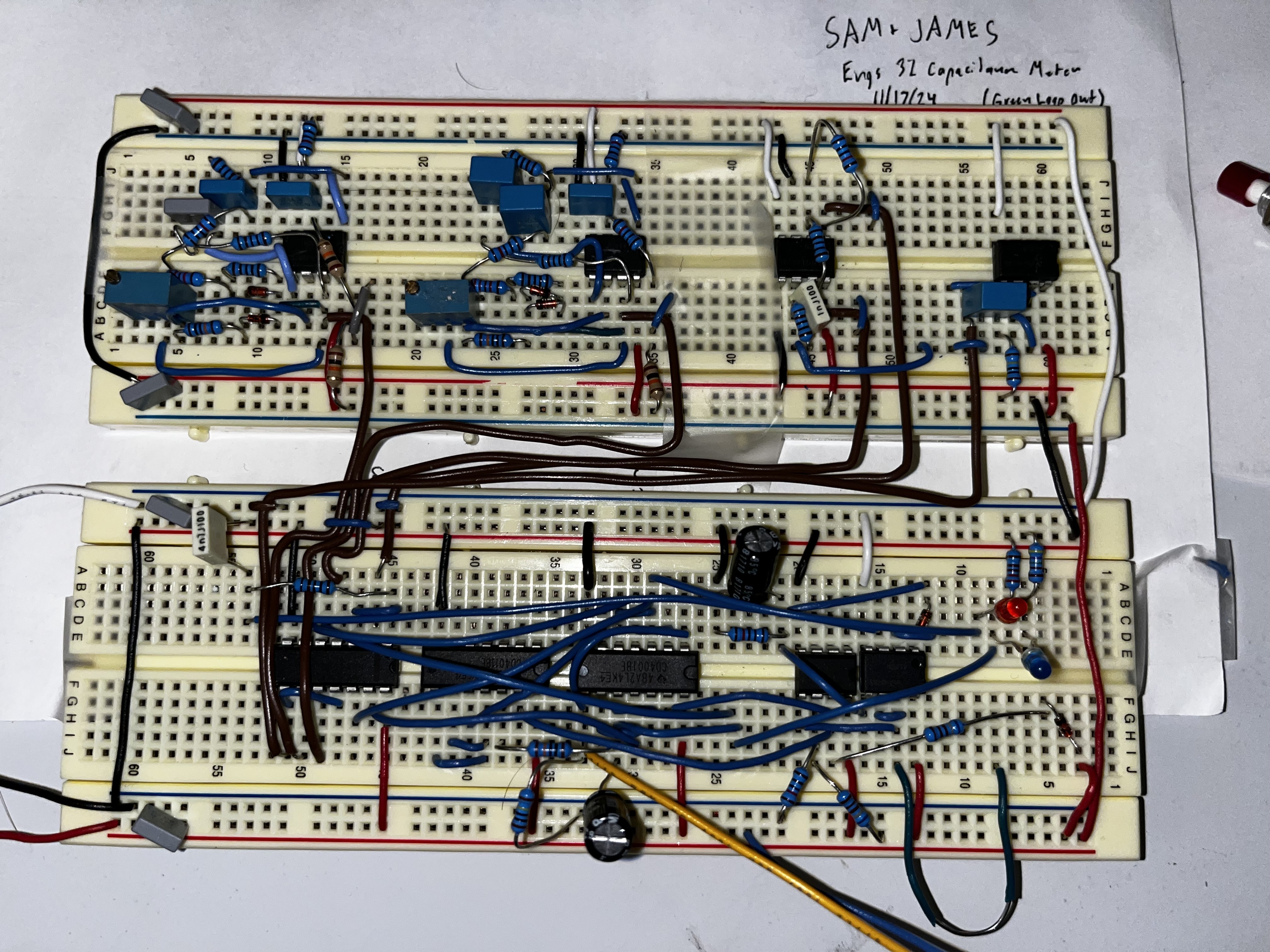
Breadboard Prototype
After verifying that the LTSpice simulations performed as expected, we moved to implement the design a breadboard with actual components.

My Partner James Attaching some Wires
We spent a lot of timee debugging on the testbench, and found several flaws when building the circuit. To name a few:
- Wires connected to wrong nodes
- Incorrect resistor values
- Incorrect capacitor values
- Too short RC delay
- Mixing up SR Latches
- Short Circuits
Final Design
Eventually we had a working final design!

Circuit with Component Blocks Overlaid
Performance
By analyzing the performance of our device, we found that the average % error was 3.8%, which is lower than the error from the capacitance manufacturers. The error was generally positive, so tuning the gain and oscillation frequency could lower the error.
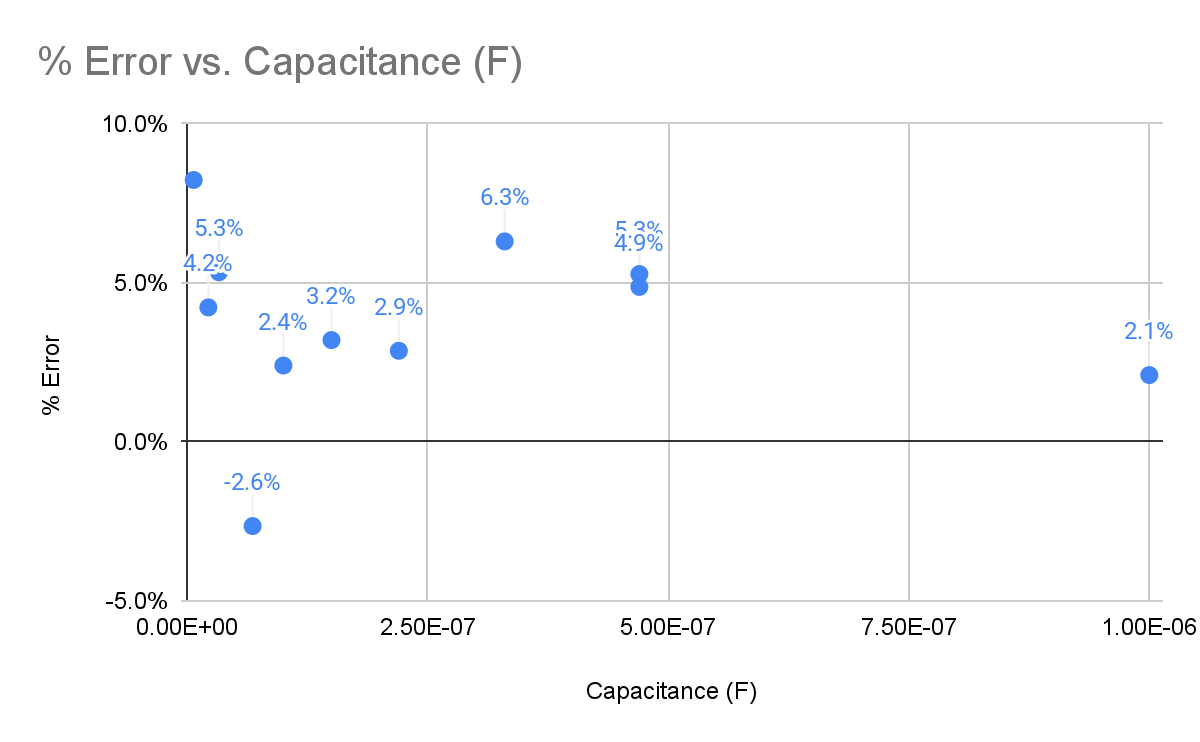
The Percentage Error for Various Capacitance Values